




Introduction
NMOS and PMOS are two types of metal-oxide-semiconductor field-effect transistors (MOSFETs). They control current through a channel by using voltage at the gate.
NMOS usually turns on with a positive gate-to-source voltage, while PMOS turns on when the gate voltage is sufficiently lower than the source voltage. Both are widely used in switching circuits, power control, and integrated circuits.
What Is NMOS?
NMOS stands for N-channel Metal-Oxide-Semiconductor. It is a transistor that uses electrons as its main charge carriers. A voltage applied to the gate creates a conductive channel between the source and drain.
In a common enhancement-mode NMOS, the transistor turns on when the gate-to-source voltage (VGS) exceeds its threshold voltage (Vth). This makes NMOS useful for switching loads, controlling current, and building digital logic circuits.

Symbol Analysis
The NMOS circuit symbol uses several lines and terminals to show how the transistor connects to a circuit.
- Gate (G): The control terminal. Its voltage controls whether a channel forms.
- Drain (D): The terminal through which conventional current usually enters an NMOS in its normal operating arrangement.
- Source (S): The terminal through which conventional current usually leaves the NMOS in that arrangement.
- Channel line: The line between the drain and source represents the controlled current path.
- Body (B): The semiconductor body terminal, shown in four-terminal symbols. It is often connected to the source in discrete MOSFETs or handled through the circuit's substrate connections in integrated circuits.
- Arrow: The NMOS body arrow points outward, away from the channel. It helps distinguish NMOS from PMOS in circuit diagrams.
What Is PMOS?
PMOS stands for P-channel Metal-Oxide-Semiconductor. It is a transistor that uses holes as its main charge carriers. Like NMOS, it controls current between the source and drain through an electrically controlled channel.
In a common enhancement-mode PMOS, the gate must be sufficiently lower in voltage than the source to turn the transistor on. PMOS devices are often used as high-side switches, where they control power supplied to a load. They also work with NMOS devices in complementary MOS (CMOS) circuits.

Symbol Analysis
The PMOS symbol contains the same basic terminals as the NMOS symbol, but its identifying features differ according to the symbol standard.
- Gate (G): The control terminal. A sufficiently low gate voltage relative to the source turns on a common enhancement-mode PMOS.
- Drain (D): The terminal through which conventional current usually leaves a PMOS in its normal operating arrangement.
- Source (S): The terminal through which conventional current usually enters the PMOS in that arrangement.
- Channel line: The line between the drain and source represents the controlled current path.
- Body (B): The semiconductor body terminal. It is commonly connected to the source in discrete PMOS devices.
- Arrow: The PMOS body arrow points inward, toward the channel.
NMOS vs. PMOS: Structure
NMOS and PMOS share the same basic MOSFET design. Both have a gate separated from the semiconductor by an insulating layer, with source and drain regions on either side. Their main structural difference is the type of channel and the semiconductor regions used to form it.
NMOS Structure
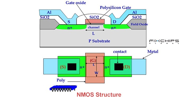
- Gate: A conductive layer, commonly polysilicon or metal, controls the channel through an electric field.
- Gate insulator: A thin insulating layer, commonly silicon dioxide or another gate dielectric, separates the gate from the semiconductor.
- Source and drain: N-type semiconductor regions supply and collect electrons during normal operation.
- Channel: An n-type conducting channel forms beneath the gate when the gate voltage is high enough relative to the source.
- Body or substrate: In a common NMOS structure, the body is p-type silicon. It supports the channel and affects the transistor's electrical behavior.
PMOS Structure
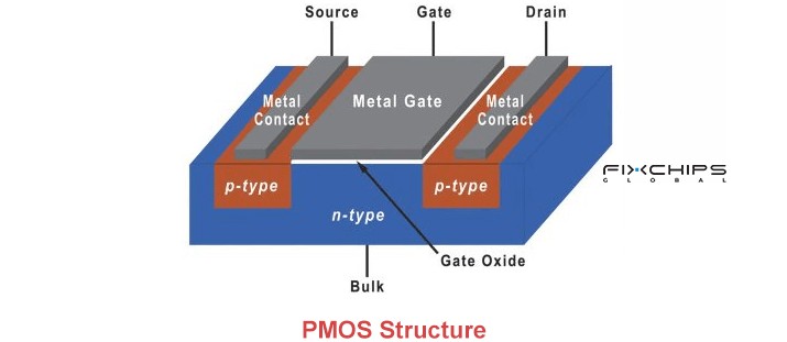
- Gate: A conductive layer controls the channel through an electric field.
- Gate insulator: A thin dielectric separates the gate from the semiconductor and prevents direct gate-to-channel conduction under normal conditions.
- Source and drain: P-type semiconductor regions supply and collect holes during normal operation.
- Channel: A p-type conducting channel forms beneath the gate when the gate voltage is sufficiently low relative to the source.
- Body or well: In a common PMOS structure, the device is built in an n-type body or well. This region supports the channel and helps isolate the transistor in an integrated circuit.
NMOS vs. PMOS: Working Principle
Both transistors use an electric field to control the channel between the source and drain. The main difference is the voltage polarity needed to form a conducting channel.
NMOS Working Principle
An NMOS turns on when its gate-to-source voltage (VGS) exceeds its threshold voltage (Vth). The threshold voltage is the gate-to-source voltage at which channel conduction begins under specified test conditions.
When VGS is below the threshold, the channel is not strongly formed, so the transistor is considered off in a basic switching model.
When VGS rises above the threshold, electrons form a conductive channel. The drain-to-source voltage (VDS) then helps determine the operating region.
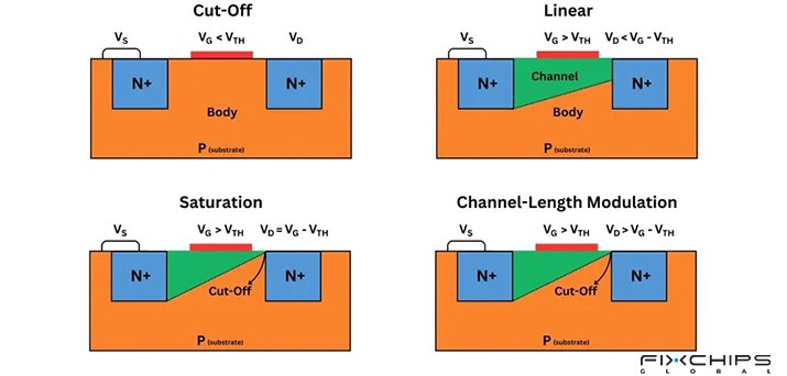
Cutoff: When VGS< Vth, the transistor is off in the basic model. The channel does not provide a normal conducting path, although small leakage current can still flow.
Linear: When VGS > Vth and VDS < VGS-Vth, the transistor is on. It behaves approximately like a voltage-controlled resistor.
Saturation: When VGS > Vth and VDS ≥ VGS-Vth, the transistor enters saturation. In the basic model, drain current is controlled mainly by the gate overdrive voltage rather than increasing directly with VDS.
PMOS Working Principle
A PMOS follows the same general principle, but its control voltages have the opposite polarity. Its threshold voltage is normally negative under the usual signed-voltage convention.
For easier comparison, VSG means the source voltage minus the gate voltage, and VSD means the source voltage minus the drain voltage. The PMOS turns on when VSG exceeds the magnitude of its threshold voltage (|Vth|).
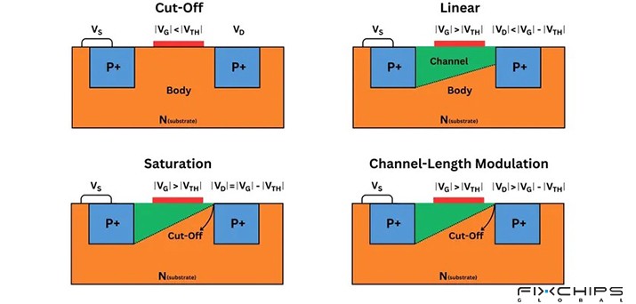
Cutoff: When VSG < |Vth|, the transistor is off in the basic model. The channel does not provide a normal conducting path, though leakage current can still occur.
Linear: When VSG > |Vth| and VSD < VSG-|Vth|, the transistor is on. It behaves approximately like a voltage-controlled resistor.
Saturation: When VSG > |Vth| and VSD ≥ VSG-|Vth|, the transistor enters saturation. In the basic model, its current is controlled mainly by the gate overdrive voltage.
NMOS vs. PMOS: Three Operating States
| Type |
Cut-off |
Linear |
Saturation |
|
NMOS | VGS < Vth |
VGS > Vth VDS < VGS-Vth |
VGS > Vth VDS ≥ VGS-Vth |
|
PMOS |
VSG < |Vth| |
VSG > |Vth| VSD < VSG-|Vth| |
VSG > |Vth| VSD ≥ VSG-|Vth| |
|
Basic Behavior |
Off; only leakage current may flow |
On; acts approximately as a controlled resistor |
Current is mainly controlled by gate overdrive in the basic model |
NMOS vs. PMOS Comparison Table
|
Feature |
NMOS |
PMOS |
|
Majority Charge Carriers |
Electrons |
Holes |
|
Substrate/Body Type |
Commonly p-type |
Commonly n-type body or well |
|
Gate Voltage to Turn ON |
Gate voltage rises above source by more than the threshold voltage |
Gate voltage falls below source by more than the threshold magnitude |
|
Operation |
n-type conducting channel |
p-type conducting channel |
|
Switching Speed |
Faster |
Slower |
|
Power Consumption | Higher | Lower |
|
Best Use |
Low-side switching, pull-down networks, and many switching applications |
High-side switching, pull-up networks, and complementary logic |
NMOS vs. PMOS: Applications
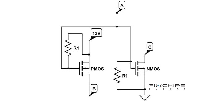
NMOS and PMOS are used in many electronic systems. Their roles often depend on where the transistor sits in the circuit and how the control voltage is applied.
NMOS Applications
- Low-side switching: An NMOS can connect a load to ground. When the gate voltage is high enough relative to the source, current flows through the load and transistor.
- Power converters: NMOS devices switch current in circuits such as buck converters. Their switching action helps control the energy delivered to the output.
- Motor control: An NMOS can switch motor current when paired with a suitable gate driver and protection components. The driver must provide enough gate-to-source voltage for the selected device.
- Signal amplification: An NMOS can amplify small input signals when biased in an appropriate operating region. Its output current changes in response to the input voltage.
PMOS Applications
- High-side switching: A PMOS can connect a power supply to a load. Pulling its gate sufficiently below its source turns it on and supplies power to the load.
- Power management: PMOS devices can control power delivery to circuit blocks. This helps a system disconnect selected loads when they are not needed.
- Battery-powered products: A PMOS can serve as a power-path switch in portable devices. Its voltage and current ratings must match the circuit requirements.
- Analog circuits: A PMOS can act as an active load or part of a current source. Its behavior depends on its bias voltage and the surrounding circuit.
How to Choose Between NMOS and PMOS
Neither type is best for every circuit. The right choice depends on the supply voltage, load current, available gate-drive voltage, switching speed, and required power loss.
|
Type |
Advantages |
Disadvantages |
|
NMOS |
|
|
|
PMOS |
|
|
Before selecting a device, check these key points:
1. Gate drive: Confirm that the available control voltage can fully turn the transistor on.
2. Current rating: Make sure the transistor can handle the expected load current.
3. On-resistance: Lower on-resistance can reduce conduction loss when the transistor is on.
4. Voltage rating: Check the maximum drain-to-source voltage and other relevant limits.
5. Heat: Estimate power loss and confirm that the package and cooling design can handle the heat.
6. Switching needs: Check switching speed, gate charge, and the requirements of the driver circuit.
For many low-side switching designs, NMOS is a practical starting point. For simple high-side switching, PMOS can be easier to control.
Complementary MOS (CMOS) Technology
NMOS and PMOS have opposite switching behavior. Combining them allows a circuit to use one transistor to pull an output low and the other to pull it high. This complementary arrangement forms the basis of CMOS technology.
What Is CMOS?

CMOS stands for Complementary Metal-Oxide-Semiconductor. It is a circuit technology that combines NMOS and PMOS transistors to perform logic and other electronic functions.
CMOS is widely used in processors, memory chips, microcontrollers, image sensors, and many other integrated circuits. One key benefit is low static power consumption in properly designed digital logic, because the complementary transistors generally avoid a direct current path from the supply to ground in stable logic states.
How Does CMOS Work?
Consider a basic CMOS inverter. It contains one PMOS transistor connected to the positive supply and one NMOS transistor connected to ground. Their gates share the same input, and their drains connect to the output.
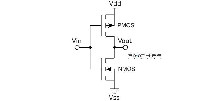
When the input is low, the PMOS turns on and the NMOS turns off. The output is pulled high. When the input is high, the PMOS turns off and the NMOS turns on, pulling the output low.
During a transition, both transistors may conduct briefly. This creates short periods of extra current and contributes to dynamic power consumption. The circuit also uses energy to charge and discharge internal and output capacitances.
Advantages of CMOS
- Low static power: Properly designed CMOS logic uses very little steady-state power.
- High integration: Many transistors can be built on a small chip.
- Good noise tolerance: CMOS logic can maintain clear high and low voltage levels within its design limits.
- Wide application range: CMOS supports digital, analog, and mixed-signal circuits.
- Efficient switching: Complementary transistor action reduces unnecessary current flow in stable logic states.
In short, NMOS and PMOS are two related but different transistor types. NMOS often suits low-side switching and fast current control, while PMOS is useful for high-side switching and pull-up paths. Together, they form CMOS circuits that power much of modern electronics.
Frequently Asked Questions
What are NMOS and PMOS?
NMOS and PMOS are two types of MOSFETs. NMOS uses electrons as its main charge carriers, while PMOS uses holes. They require opposite gate-to-source voltage polarities to turn on in enhancement mode.
How to identify NMOS or PMOS?
Check the component's part number and datasheet to confirm its channel type. You can also examine the circuit symbol: in a common four-terminal symbol convention, the body arrow points inward for NMOS and outward for PMOS.
Is NMOS faster than PMOS?
NMOS is often faster than PMOS under similar conditions. Electrons generally move more easily through silicon than holes.
Is NMOS normally on or off?
A common enhancement-mode NMOS is normally off when its gate-to-source voltage is zero, so it behaves like an open switch in a basic circuit model.
A depletion-mode NMOS is normally on at zero gate-to-source voltage, so the default state depends on the transistor type.
Why is PMOS larger than NMOS?
In CMOS circuits, PMOS transistors are often made wider than NMOS transistors because holes generally have lower mobility than electrons in silicon. A wider PMOS can help provide similar drive strength and balance the switching performance of the two transistors
Related Articles


