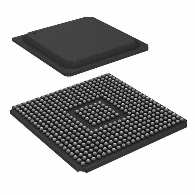
Xilinx XC2V1000-6FG256C

Image is only for reference













| Attribute | Value |
|---|---|
| PPAP | No |
| SVHC | Yes |
| EU RoHS | Not Compliant |
| Mounting | Surface Mount |
| ECCN (US) | EAR99 |
| Pin Count | 256 |
| Tradename | Virtex |
| User I/Os | 172 |
| Automotive | No |
| Lead Shape | Ball |
| Family Name | Virtex-II |
| PCB changed | 256 |
| Speed Grade | 6 |
| Availability | No Stock Available |
| JTAG Support | Yes |
| Package Width | 17 |
| Logic Elements | 11520 |
| Package Height | 1.4(Max) |
| Package Length | 17 |
| Copy Protection | No |
| I/O Voltage (V) | 1.5|3.3|1.8|2.5 |
| Programmability | No |
| Shift Registers | Utilize LUT |
| Supplier Package | FBGA |
| Device Logic Gates | 1000000 |
| Device Logic Units | 11520 |
| Process Technology | 0.15um |
| Device System Gates | 1000000 |
| Number of I/O Banks | 8 |
| Number of Registers | 10240 |
| Program Memory Type | SRAM |
| Opr. Frequency (MHz) | 820 |
| Number of Multipliers | 40 (18x18) |
| Standard Package Name | BGA |
| Embedded Memory (Kbit) | 720 |
| SVHC Exceeds Threshold | Yes |
| Maximum I/O Performance | 840Mbps |
| Number of Global Clocks | 16 |
| In-System Programmability | Yes |
| Reprogrammability Support | Yes |
| Supplier Temperature Grade | Commercial |
| Maximum Supply Current (mA) | 250 |
| Maximum Distributed RAM Bits | 163840 |
| Operating Supply Voltage (V) | 1.5 |
| Number of Inter Dielectric Layers | 8 |
| Total Number of Block RAM Memories | 40 |
| Maximum Operating Temperature (°C) | 85 |
| Minimum Operating Temperature (°C) | 0 |
| Maximum Operating Supply Voltage (V) | 1.575 |
| Minimum Operating Supply Voltage (V) | 1.425 |
Purchase & Inquiry
You can place an order with FIXCHIPS without having to register or create an account.
To make payment more convenient, we support multiple payment methods in USD, including PayPal, credit cards, and wire transfer.
We suggest submitting an RFQ to get the most up-to-date pricing and availability for the components you are looking for. Our sales team will reply by email within 24 hours.
1. An email containing your order details will be sent to your inbox. If you cannot find it, please check your spam or junk mail folder.
2. Product availability and pricing may change over time. Our sales manager will verify the details of your order and contact you if any changes or confirmation are required.
Packaging Process